|
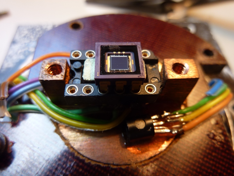
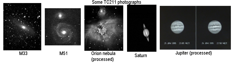
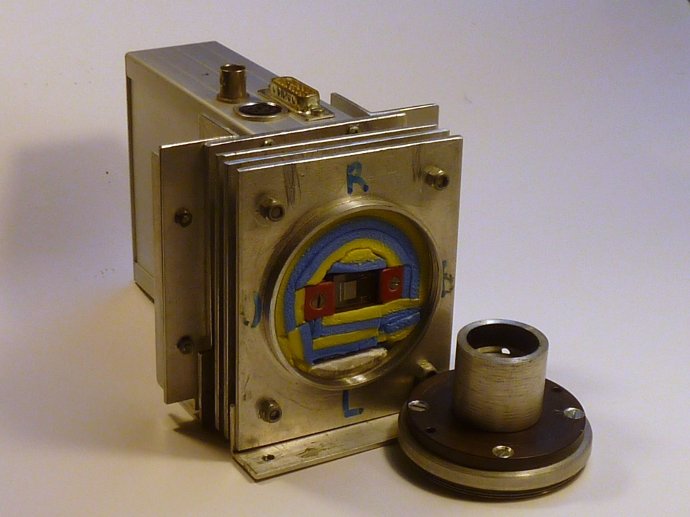
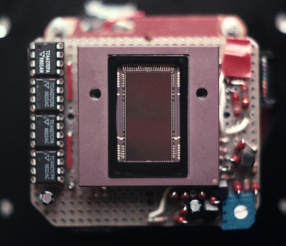
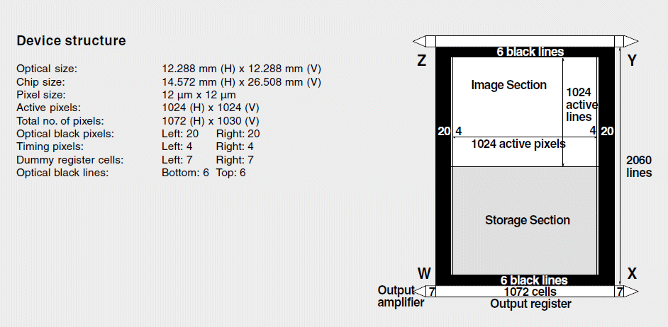
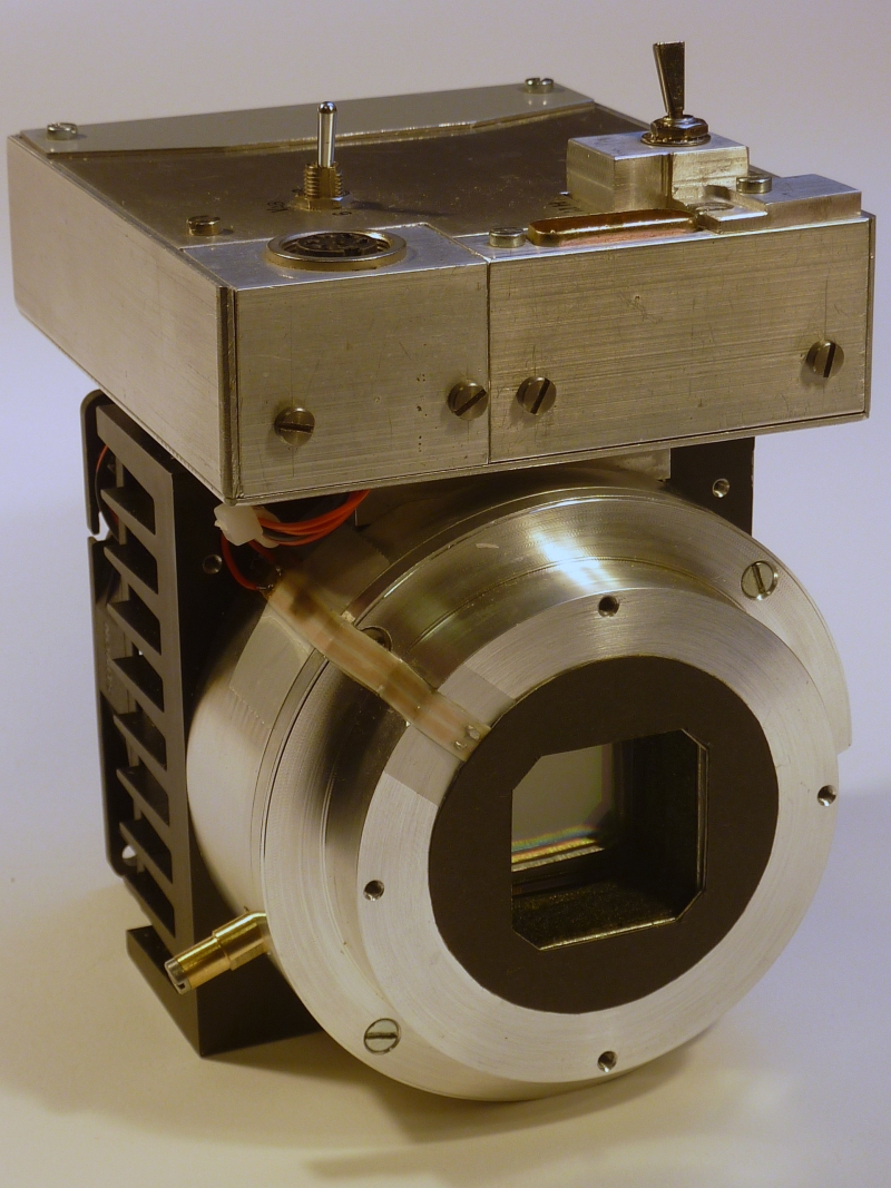
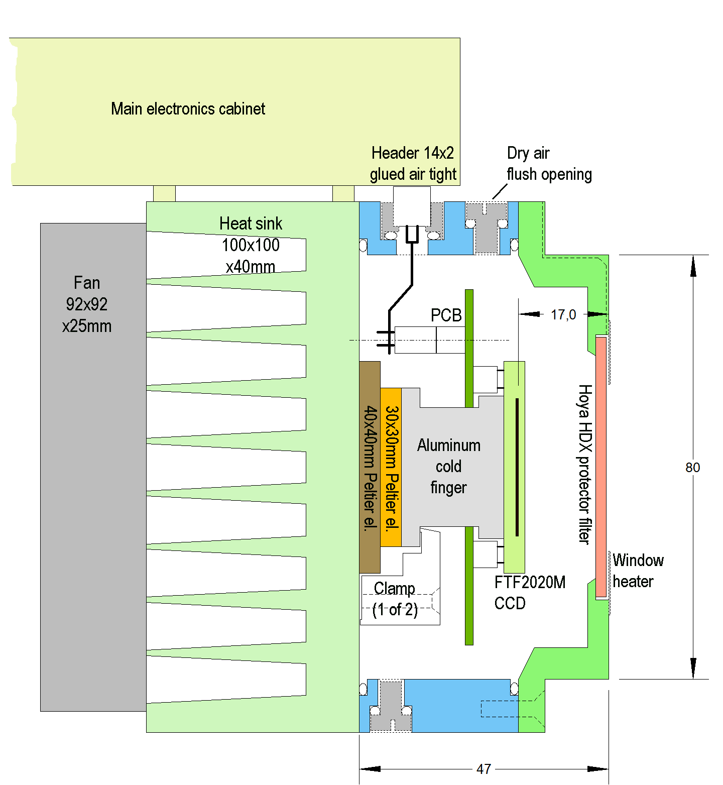
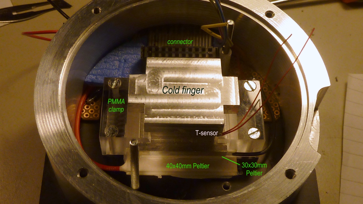
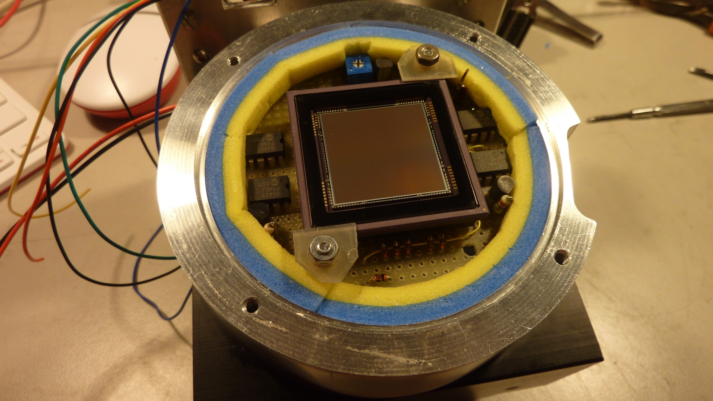
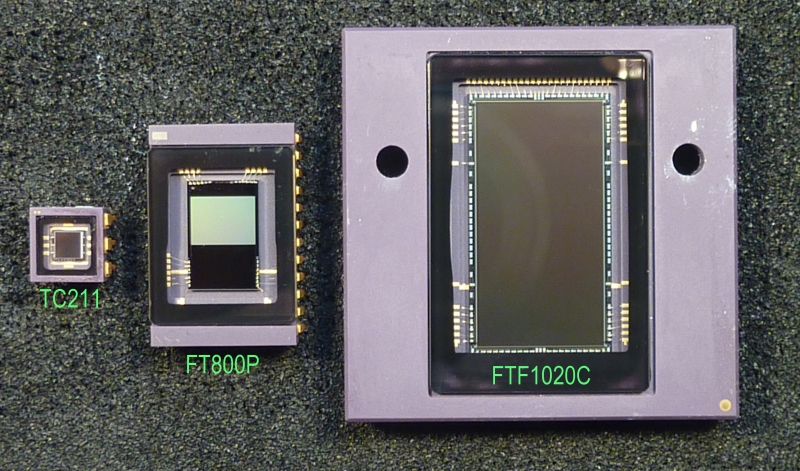
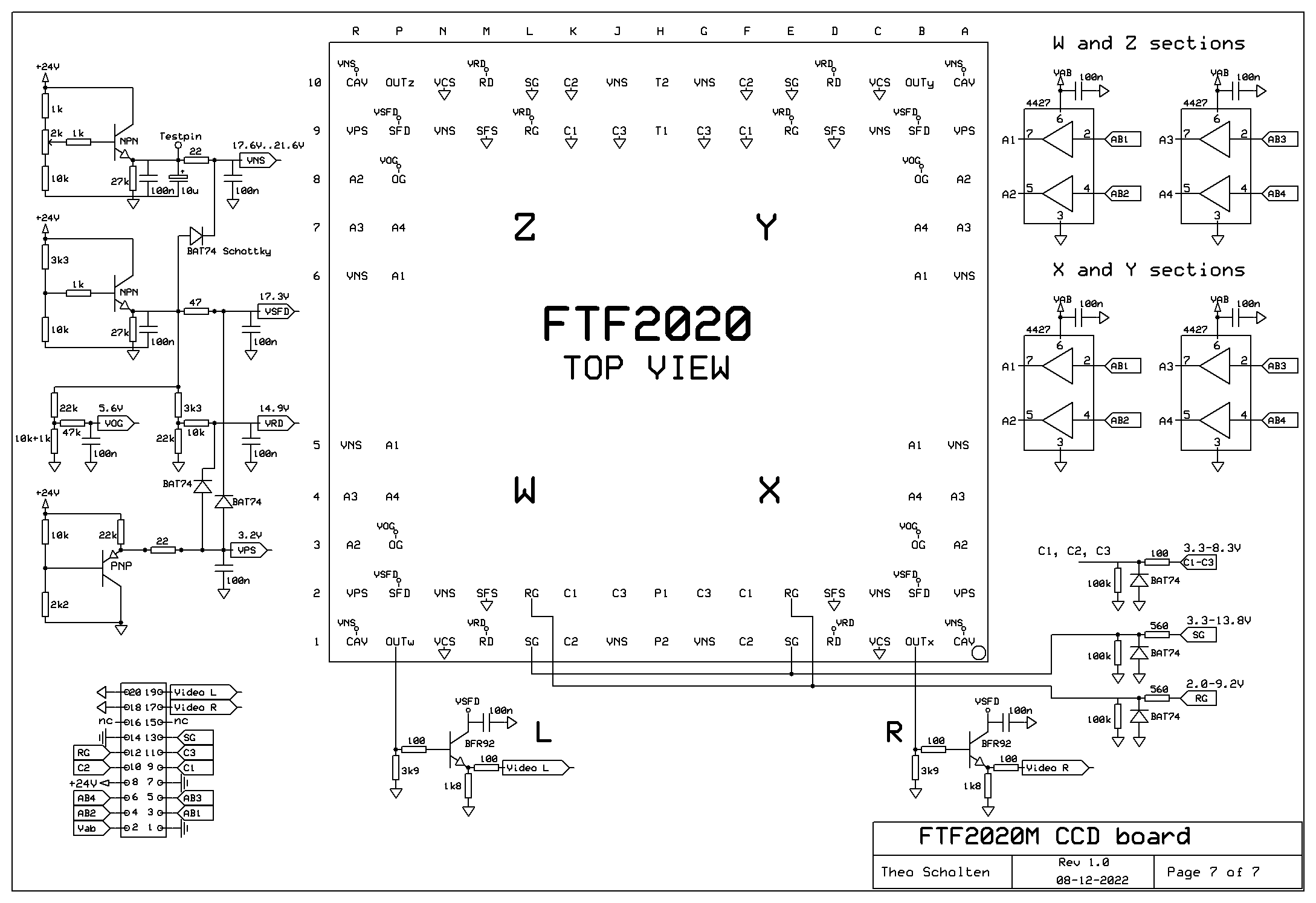
Out-of-use camera's: I designed and built my first CCD-camera in 1994 based on a Texas Instrument, full-frame CCD, the TC211, with 195x165 pixels of 13.8x16um (sensitive area: 2.6x2.6mm). Only a limited number of TC211-photographs remain from this initial period. In 1996 I got hold of a Philips FT800P frame-transfer chip with a sensitive area of 6.4x4.8mm and 734x580 pixels (HxV). The chip was used in a non-interlaced mode and horizontal binning, resulting in 367x290 pixels of 17.0x16.8um. These camera's are out of use. Currently used camera's: In 1999 I received an FTF1020-C colour CCD chip from Philips Nat-lab and early 2002, after discussing with them the set-backs of a colour chip for astrophotography, Philips surprised me by sending an FTT1010-M and FTF2020-M monochromatic chip. (Shortly thereafter this CCD-line was transferred to Dalsa. ) Running out of possibilities and connections to obtain single CCD- (or CMOS-) chips, I'm still using these two CCD's, up to this date! The FT-line of chips uses standard 1kx1k buiding blocks to manufacture CCDs with different sizes and aspect ratios but with functionaly identical shift registers and output circuitry. Pixels measure 12x12um. The FTT-type is a frame transfer model with a light schielded storage section that can operate without shutter; the FTF-type is a full-frame version. Images below are of the recently (2022) upgraded FTF2020-M camera, featuring a 2-stage Peltier stack for improved cooling and lower dark current. |
 |
 |
 |
 |
 |
 |
|
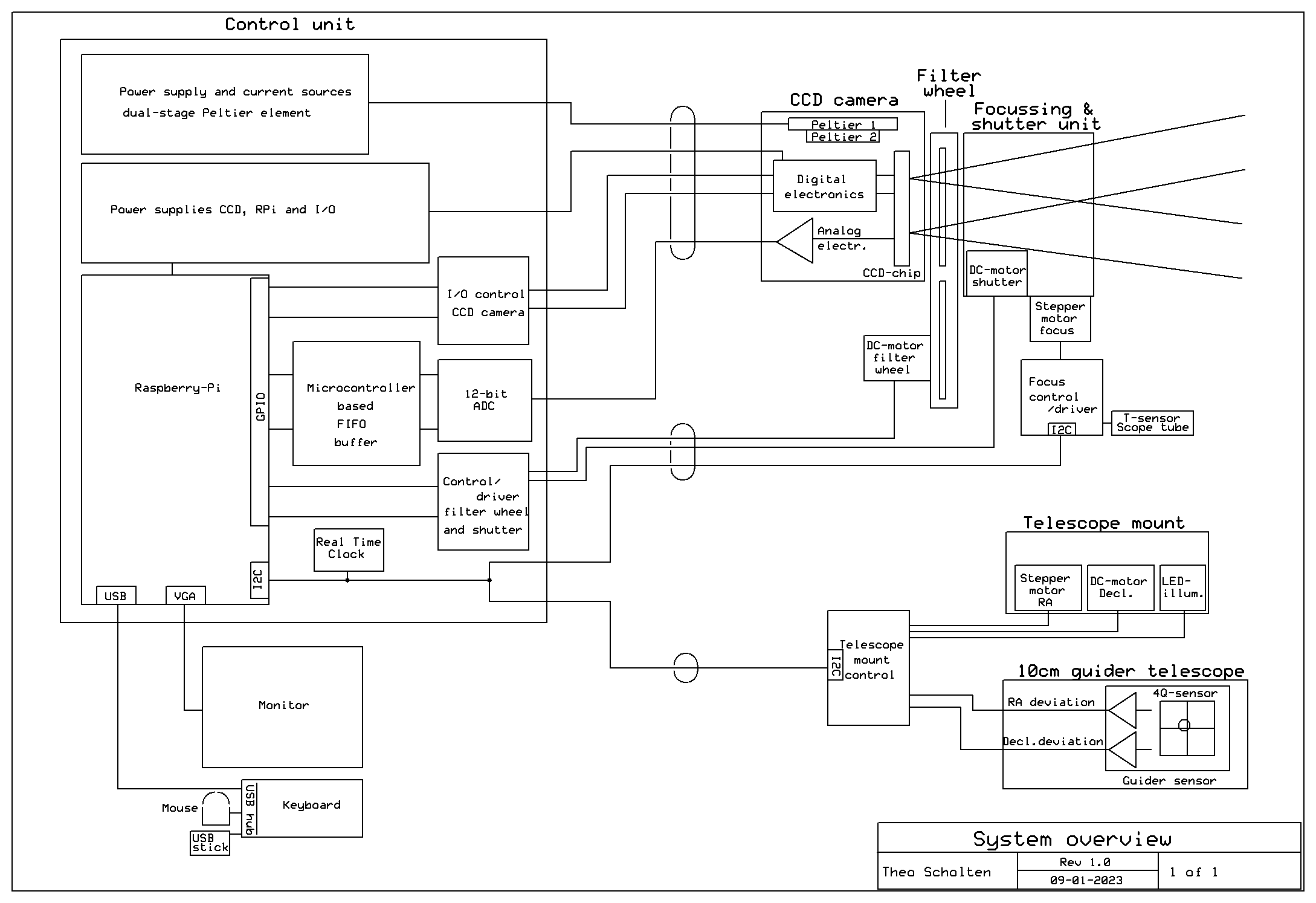
The basic design, construction and electronics of the camera's holding these CCD's are similar to the TC211 and FT800P camera's:
Digital part: The electronics board of the camera mainly comprises digital circuits with the following functions (IO's):
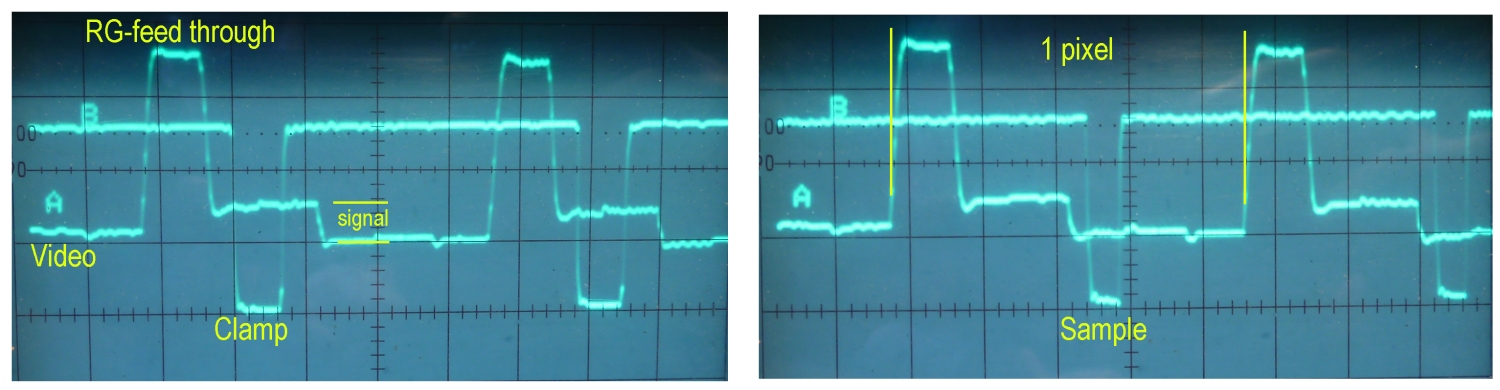
A small part of the camera-board consists of an analog circuit for processing the video signal. It contains a low noise, AC-coupled AD797 opamp that, using an external switch, provides a gain of 4x, 11x or 32x. The output of the Opamp is connected to a sample-and-hold circuit that uses Correlated Double Sampling: Every pixel-cycle, after charge reset, clamp the output signal to ground before sensing the video signal of that pixel. The S&H output is fed to the 12-bit (0..4096) analog-to-digital convertor of the 'system controller' . Find TI, Philips and Dalsa CCD data sheets here! |